Low-Energy Electron Diffraction (LEED)
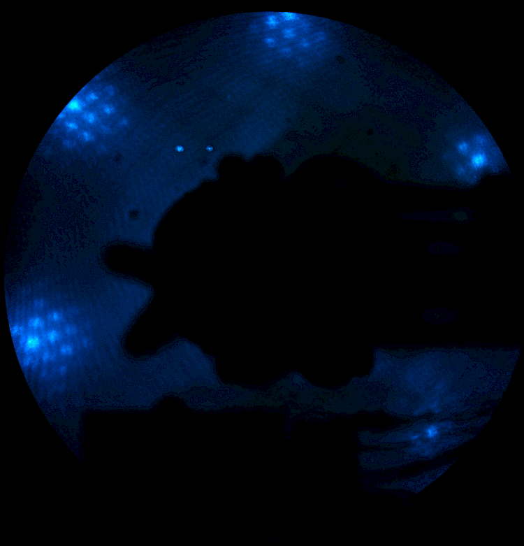
In LEED a beam of electrons, with energy of the order of 100 eV, is diffracted at the lattice of the sample. Because of the low mean free path of electrons with energies in this range most of the diffraction happens at the topmost lattice planes, making the technique surface-sensitive. We use LEED to identify ordered phases of adsorbed particles, to characterize the degree of order, and to do structure analysis of adsorbate phases.

Figure: LEED of a graphene layer on a Ru(0001) surface. The hexagonal arrangement of diffraction spots reflects the symmetry of the surface (some of the diffraction spots are hidden by the sample manipulator). The closely-spaced satellite spots are caused by a superstructure with a lattice constant of approximately 30 Å. It is caused by the lattice mismatch of graphene and Ru(0001), giving rise to a moiré effect. Reprinted with permission from "Scanning tunneling microscopy of graphene on Ru(0001)", S. Marchini, S. Günther and J. Wintterlin, Phys. Rev. B 2007, 76, 075429. Copyright 2007, American Physical Society.